Muntasir Mahdi – Portfolio
| _Virginia Tech | Auburn University_ |
Graduate Projects
Optical and Electronic Properties of Epitaxial Germanium
Optical characterization, modeling, and strain-dependent transitions in epitaxial Ge and GeSn thin films.
Overview
This research examines the
- optical and electronic behavior of epitaxial Ge and GeSn thin films for photonics and quantum devices, using spectroscopic ellipsometry, and critical-point (CP) analysis.
- How strain, defects, buffer layer thickness, and substrate orientation modulate the dielectric response and band-structure transitions.
1️⃣ Optical Constants and Critical-Point Transitions in Biaxially Tensile-Strained Ge
Phys. Rev. Applied 23, 024037 (2025)
DOI: 10.1103/PhysRevApplied.23.024037
- Comprehensive ellipsometry modeling of biaxially strained epitaxial Ge films grown by molecular beam epitaxay (MBE).
- Strain-induced shifts in Critical Point transitions were extracted via second-derivative CP analysis, linking strain and film thickness to dielectric evolution.

Key Findings:
- Extracted full (n, k) and (ε₁, ε₂) spectra for strained Ge.
- Developed a multi-layer optical model including surface and oxide effects.
- Established strain–band-structure correlation for Si-compatible photonics.
Methods
- Spectroscopic Ellipsometry (0.4–4.5 eV)
- Critical-Point Analysis
Related Publications
- Optical constants and critical-point transitions in biaxially tensile-strained epitaxial thin films of germanium
Rutwik Joshi, Nina Hong, Neha Singh, Muntasir Mahdi, and Mantu K. Hudait Phys. Rev. Applied 23, 024037 (2025)
DOI: 10.1103/PhysRevApplied.23.024037 - Impact of defects, buffer layer thickness, and substrate orientation on optical properties of epitaxial germanium (Under Review) Muntasir Mahdi, Nina Hong, Neha Singh, Mantu K. Hudait
NbN Superconducting Resonator for Strong Magnon–Photon Coupling
Fabrication and measurement of NbN superconducting resonators demonstrating strong coupling with YIG spheres.
Superconducting resonators enable strong interactions between microwave photons and magnons, forming a key platform for hybrid quantum systems. This project demonstrates:
- NbN microstrip resonators integrated with yttrium iron garnet (YIG) spheres to realize strong magnon–photon coupling at cryogenic temperatures.
- The DC lines and Indium bumps were aimed for current-controlled magnon–photon coupling.
- Details of the electroplating are described on CPW Fabrication and Electroplating Indium.
Design and Fabrication
- I designed meander-type microstrip NbN resonators (10 mm × 5 mm) optimized for magnetic-field-dependent coupling experiments.
- I have fabricated the devices on intrinsic Si substrates (525 µm thick) with 250 nm NbN traces deposited by DC reactive sputtering.
- Al contact pads were added for microwave wirebonding, and a NbN backside ground plane completed the structure.


Measurement and Characterization
- The assembly was tested in a Quantum Design PPMS for cryogenic and magnetic-field measurements.
- A VNA (Agilent N5227A) was used to perform S-parameter measurements (S₁₁, S₂₁) from 100 MHz – 30 GHz at 1.8 K.
- An in-plane and out-of-plane magnetic field was applied to drive the YIG into ferromagnetic resonance (FMR) and observe magnon–photon hybridization.


Bottom: Corresponding Q-factors of a resontor with and without the YIG sphere.
Reprinted with permission from M. Mahdi et al., IEEE Trans. Appl. Supercond., vol. 35, no. 5, Aug 2025. © IEEE.
Key Results
- At 1.8 K, the system exhibited clear avoided crossing in the S₂₁ spectra, confirming strong coupling between microwave photons and magnons.
- These results establish a scalable pathway toward hybrid quantum magnonic devices based on superconducting circuits.
“Hybrid systems like NbN–YIG platforms bridge the gap between superconducting quantum circuits and magnonic information carriers.”
Acknowledgment
This research is supported by the Air Force Office of Scientific Research (AFOSR) under grant funding for hybrid quantum systems.

Superconducting Nb & Cu Resonator/CPW Fabrication
Microfabrication of superconducting Nb resonators/ CPWs for cryogenic measurements and Cu resonators/ CPWs for room-temperature testing.
Overview
For multiple projects I have done the fabrication and characterization of:
- Nb resonators and CPWs for low-temperature, cryogenic experiments
- Cu resonators and CPWs for room-temperature S-parameter testing
The key components of this work:
- Electroplating Indium (In) bump structures on resonator & coplanar waveguide (CPW) chips for spin pumping and magnetic control interfaces. Details in Electroplating.
- DC lines enabled current-controlled magnon–magnon and magnon–photon coupling in hybrid quantum systems.
- Established a repeatable fabrication workflow and validate resonator performance across temperatures and magnetic fields.


Fabrication Process
Devices were fabricated using optical lithography and thin-film deposition:
- Substrates: High-resistivity double sided polished Si wafers
- Deposition: DC sputtering of Nb (200 nm), and Cu (150 nm)
- Patterning: UV lithography, lift-off for Cu and Nb
- Geometry: Quarter-wave CPW resonators (50 Ω feedline, λ/4 open stub)
- Indium Bumps: Electroplated onto patterned trenches to create low-resistance current injection contacts for tunable coupling experiments
- Packaging: Wire-bonded to custom PCBs for VNA measurements
Measurements
Room-Temperature (Cu): S-parameter and impedance characterization using a VNA.
Low-Temperature (Nb): Cryogenic measurements of S21 and Q-factor at 1.7 K, demonstrating high-quality resonator performance and compatibility with hybrid magnonic architectures.
 and corresponding Q-factors (b)")
Electroplating Indium (for CPW chips)


Key Outcomes
- Established a reproducible fabrication workflow for Nb and Cu resonators/CPWs
- Developed indium bump integration for current-driven magnon–magnon and magnon–photon coupling
- Verified resonator performance trends across magnetic fields
- Provided a baseline for cryogenic hybrid quantum experiments
- Integrated Microwave Simulation → Mask/ PCB Design → fabrication → measurement pipeline
Tools & Methods

- Software: Keysight ADS, KLayout, Python
- Equipment: DC sputter system, mask aligner, VNA, optical profiler, electroplating setup
- Collaboration: Supervised by Dr. Michael Hamilton, conducted at Alabama Micro/Nano Science and Technology Center
Electroplating Indium for Current-Controlled Magnon–Photon Coupling
Electroplating of indium bumps on Nb and NbN coplanar waveguides and resonators for flip-chip bonded current-controlled magnon–photon coupling measurements.
This project developed a
- Nb and NbN coplanar waveguide (CPW) platform with indium bump electroplating for flip-chip bonded, current-controlled magnon–photon coupling experiments.
- The DC lines and indium bumps enable current injection (spin pumping) across magnetic samples, allowing tunable hybrid interactions in cryogenic measurements.

Electroplating Process
- Indium bumps were electroplated at predefined contact pads on Nb and NbN DC lines using a pulsed DC electroplating process with a Ti/Cu seed layer for conductivity and adhesion.
- Deposition parameters were optimized for uniform thickness (~10–15 µm), low roughness, and excellent mechanical stability during flip-chip alignment.
- Module used: HP Hewlett Packard 8011A Pulse Generator

Flip-Chip Integration and DC Lines
- The electroplated indium bumps were designed for flip-chip bonding with magnetic or hybrid samples containing DC bias lines for current control.
- These bonded structures enable dynamic modulation and spin pumping of the magnon–photon coupling strength by injecting DC bias through the superconducting paths.

Connection to Related Work
This electroplating process supports the Nb and NbN superconducting resonator, coplanar waveguides project used for magnon-magnon and magnon–photon coupling studies. Details of the resonator design and measurement setup are described on NbN Resonators.
Acknowledgment
This research is supported by the Air Force Office of Scientific Research (AFOSR) under grant funding for hybrid quantum systems.
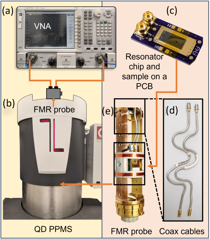
Magnetic & Structural Characterization
Measurement and analysis of magnetic and nanoscale properties using PPMS, VNA, AFM/MFM, XRD, and related instruments. Many of the PPMS measurements were done at low temperature (sub 2 K).
Different project goals were involved characterization of magnetic and structural properties of materials using:
- PPMS Measurements: Magnetic (VSM), ferromagnetic resonance (FMR), electrical transport (ETO), Hall Measurement and current-dependent measurements using Keithley 6221 and NV 2182.
- RF & VNA Measurements: Frequency vs. magnetic field S21 characterization using Vector Network Analyzer (VNA).
- Lock-In Amplifier & RF Generator: Signal detection and excitation for magnetic and transport experiments.
- Structural & Surface Analysis: X-Ray Diffraction (XRD) for crystal structure, Atomic & Magnetic Force Microscopy (AFM/MFM) for topography and magnetic domain imaging.
Reprinted with permission from M. Mahdi et al., IEEE Trans. Appl. Supercond., vol. 35, no. 5, Aug 2025. © IEEE.
Reprinted with permission from M. Mahdi et al., IEEE Trans. Appl. Supercond., vol. 35, no. 5, Aug 2025. © IEEE.
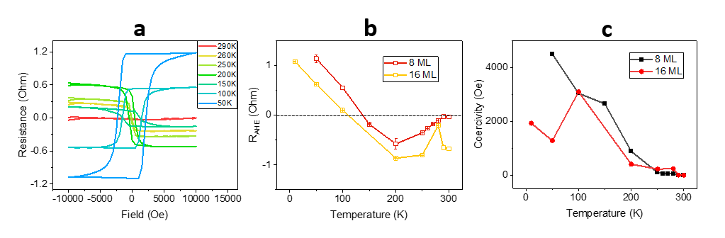
These results for CrTe2 sample I presented at MMM-Intermag 2022 Conference .
These measurements enabled quantitative analysis of magnetic, electrical, and structural properties at the nanoscale, facilitating material optimization and device performance evaluation.
Python Automation for PPMS–VNA and Transport Measurements
Python-based programming to automate measurements with synchronized magnetic field, temperature, and frequency sweeps using PPMS, Agilent PNA 5227A, and Keithley instruments.
⚙️ Project Overview & Motivation
I have developed a Python automation suite for synchronized magnetic-field, temperature and frequency-dependent measurements using:
- Quantum Design PPMS,
- Agilent PNA 5227A, and
- Keithley 6221/2182A instruments.
🧪 The software automates:
- FMR (Ferromagnetic Resonance): frequency–field mapping to extract resonance fields, linewidths, and effective damping.
- Electrical Transport Option (ETO): Temperature- and field-dependent Hall, and magnetoresistance data collection.
- Frequency-vs-field S21 measurements: microwave measurements by synchronizing with VNA
It replaced an expensive commercial packages and saving over $4,000.
 sweep using Python")

🧩 Technical Implementation
![]()
- Language: Python (v3.11)
- Communication Protocols:
- GPIB and VISA (via
pyvisa) - Quantum Design API for PPMS control
- GPIB and VISA (via
- Supported Instruments:
- Agilent PNA 5227A (S11, S21 scattering measurements)
- Keithley 6221 (current source) and 2182A (nanovoltmeter)
- PPMS DynaCool (field, temperature)
- Core Libraries:
numpy,matplotlib,pandas,pyvisa,scipy - Features:
- Frequency sweep automation with synchronized field ramping
- Temperature-stabilized measurement loops
- Multi-scan averaging and noise filtering
- CSV output for post-processing and plotting
- Modular GUI-free design for remote execution
💻 Code Access
Full source code and example datasets are available on GitHub:
Repositories include ready-to-use command templates, VISA initialization scripts, and sample measurement logs for PPMS setups.
Material Deposition and Characterization (YIG, Permalloy, Cu, Ti, Pt etc)
Thin-film deposition and characterization of materials (metals, dielectrics, magnetic), annealing, AFM, VSM, XRD among other analyses.
Overview
I have done deposition and characterization of magnetic thin films, specifically Yttrium Iron Garnet (YIG) and Permalloy (Ni₈₀Fe₂₀), and other materials such as Cu, Ti, Pt for use in magnonic, spintronic, optoelectronic and MOS devices.
I utilized RF and DC sputtering followed by annealing, and performed AFM, vibrating sample magnetometry (VSM), etc**, and **XRD crystallographic verification**.
YIG and Permalloy Thin-Film Deposition
YIG and Permalloy films were deposited using a single-target sputtering system under controlled pressure and power conditions. Below are some sputtering parameters, they can vary vastly depending on specific sputtering chamber/setup.
- YIG deposition: RF sputtering on GGG or Si substrates
- Permalloy deposition: DC sputtering on Si/SiO₂ substrates
- Base pressure: 3 × 10⁻⁶ Torr
- Working pressure: 5 mTorr in Ar
- Power: 70-80 W (RF), 60 W (DC)
- Tips and Tricks:
- Using Cu backing plate with YIG target minimize the risk of target cracking.
- Use 20 mils thick permalloy target instead of 0.25” thick target. Because, thicker target have difficulty striking the plasma due to strong ferromagnetism of permalloy.


Surface Morphology and Annealing
- Deposition thickness of YIG films was inspected using Atomic Force Microscopy (AFM).
- To crystallize the amorphous YIG layer, samples were annealed at 850 °C for 3–4 hours in ambient oxygen, followed by controlled cooldown to room temperature.


Magnetic and Structural Characterization
After annealing, films were characterized using Vibrating Sample Magnetometry (VSM) and X-ray Diffraction (XRD):
- VSM: Measured in-plane (IP) and out-of-plane (OOP) hysteresis (M–H) loop, revealing magnetic hysteresis and low coercivity.
- XRD: 2θ–ω scans confirmed polycrystalline YIG peaks and phase purity after high-temperature annealing.


Additional Fabrication Work
- Sputtering deposition of Ti, Cu, Pt, Al, TiN, and other metallic layers for device contacts
- ALD growth of Al₂O₃ for dielectric isolation and surface passivation
- Integration of multilayer stacks combining magnetic, metallic, and dielectric films
- Optimization of thickness control, adhesion, and uniformity across different substrates
- Supported process development for hybrid magnonic, photonic, and spintronic device fabrication
Tools & Facilities
- Sputtering System: KJLC RF/DC sputter tool
- Characterization: AFM, QD-PPMS (VSM), and Rigaku XRD
- Annealing Furnace: High-temperature furnace (1200 °C max)
- Location: Alabama Micro/Nano Science and Technology Center and VT ECE Micron Technology Semiconductor Processing Lab
Nb Josephson Junction Fabrication
Fabrication and characterization of Nb/AlOx/Nb Josephson junctions.
The Nb Josephson Junction (JJ) devices were fabricated using:
- A multilayer stack structure of Al pad / Nb / AlOx / Nb / SiO2 / Si substrate.
- The process involved thin-film deposition, oxidation, E-beam lithography and photolithography steps.


These junctions form the fundamental building blocks for superconducting qubits and microwave resonator coupling experiments, enabling precise studies of quantum coherence and nonlinear dynamics at millikelvin temperatures.
PCB Design & Assembly for Sub-2 K Magnetic Measurements
PCB assembly, CPW mounting, and low-temperature setup for magnetic sample characterization.
I have designed and assembled PCBs for low-temperature (<2 K) magnetic measurements.
- Careful orientation of in-plane (IP) and out-of-plane (OOP) samples, coaxial cable routing, and current pad layout for high-precision experiments.
- Creating SMP port and pin footprints
- 4-layer design for DC lines connections using pads, via and pins
- Assembly steps: SMP port integration, CPW and resonator chip mounting using conductive silver paint, and curing for stable low-temperature operation.


Key Steps & Techniques
![]()
- PCB Design: Layout for current application pads and coax routing optimized for low-temperature operation. (Designed using: Altium Designer)
- Sample Orientation: In-plane (IP) and out-of-plane (OOP) mounting for magnetic characterization.
- Chip Assembly: CPW and resonator chips mounted with conductive silver paint, followed by curing in a vacuum oven.
- Connector Integration: SMP ports soldered using solder paste for robust RF connections.
- Sub-2 K Measurement Preparation: Assembled boards are compatible with cryogenic measurement setups for magnetic samples.


Demonstrated precision PCB assembly techniques for low-temperature magnetic experiments, combining RF design, mechanical mounting, packaging and cryogenic compatibility.
High-Vacuum Ion Milling System Setup and Commissioning
Complete setup, calibration, and operation of a Kaufman Ar ion milling system for precision surface processing.
In this project I have done:
- The complete setup, calibration, and commissioning of a high-vacuum ion milling system for advanced material processing and ferromagnetic thin-film research.
- I was solely responsible for the mechanical assembly of the CF flanges, vacuum configuration, and operational testing of the entire system — including pump integration, Ar flow control, and ion beam source tuning.
- I acknowledge AMNSTC Lab manager (Drew Sellers) for helping out with troubleshooting.


 and control panels")
⚙️ System Specifications
| Component | Specification / Model | Description |
|---|---|---|
| Ion Source | Kaufman & Robinson KDC-40 | Argon ion source for material etching and surface modification |
| Ion Source Controller | KRI KSC-1202 | Power supply and control of beam and discharge parameters |
| Turbo Pump | Pfeiffer HiPace300 | High-speed turbomolecular pump (1000–1005 Hz normal operation) |
| Backing Pump | Edwards Dry Pump | Supports turbo pump during chamber evacuation |
| Chamber Base Pressure | ~5 × 10⁻⁶ Torr | Achieved using turbo + dry pump configuration |
| Gas Flow System | MKS Mass Flow Controller (MFC) | Controls Ar flow rate and pressure stability |
| Ar Source | High-purity Argon Cylinder | Supplies controlled Ar flow to the ion gun |
| Valves | CF, GV valves (manual) | Isolation of chamber, turbo, and venting lines |
| Sample Holders | Custom 3D-printed (Fusion 360) | Designed for precise sample mounting and alignment |
| Control & Monitoring | KRI Beam Controller, MKS Readout | Full control over beam discharge and Ar flow |
🧩 My Role & Achievements
- Full System Setup: Assembled, and aligned the vacuum chamber, turbo, and ion source.
- Vacuum Commissioning: Achieved stable base pressure below 5×10⁻⁶ Torr.
- Custom Sample Fixtures: Modeled and 3D-printed holders in Fusion 360 for accurate sample positioning.
- Standard Operating Procedure: Authored a detailed SOP covering operation, safety, and maintenance (including ion filament replacement).
- Safety & Maintenance: Implemented proper valve sequencing and pump protection to avoid overpressure damage.


🧠 Learned Skills
- High-vacuum system design, operation, and troubleshooting
- Ion beam physics and ion milling process development
- Integration of vacuum pumps, flow control, and beam power systems
- 3D CAD-based mechanical design (Fusion 360)
- Writing and implementing Standard Operating Procedures (SOPs)
— System commissioned and operated by Muntasir Mahdi (April 2023)
Points of contact: Drew Sellers (jas0149@auburn.edu) · Mike Hamilton (mchamilton@auburn.edu)
Undergraduate Projects
Building a Mars Rover
Design and development of an autonomous Mars Rover for international robotics challenges.
- This team project involved the design and fabrication of a fully functional Mars Rover prototype capable of autonomous navigation, remote operation, and terrain adaptability.
- It was part of the University Rover Challenge (URC) 2015, Utah, USA, and later the European Rover Challenge (ERC) 2016, Jasionka, Poland — both focused on advancing planetary exploration robotics.
🚀 Overview
Between 2015 and 2017, our interdisciplinary team at the Shahjalal University of Science & Technology (SUST) developed a rover integrating mechanical, electronic, and control subsystems for rough Martian terrain.
I contributed primarily to:
- Motor driving circuitry for precision wheel and arm control
- Power distribution and sensor integration (relays and wiring); soldering.
- Mechanical chassis development for stable motion on variable slopes; used heavy cutting, drilling and grinding tools.
- Testing and debugging for field performance and remote operation
🎥 Project Demonstration
🔧 Fabrication & Team


🧭 Competition & Achievements
- University Rover Challenge 2015, Utah, USA – Qualified for Critical Design Review (CDR) stage
- European Rover Challenge 2016, Poland – Selected for final competition round
Building a Mars Rover helped us better understand how to bring together control systems, mechanics, and real-world testing.
🧩 Funding & Support
This project was partially supported by the Shahjalal University of Science & Technology Research Center (SUSTRC), Sylhet, Bangladesh.
Characterization of Carbon Nanotube Field-Effect Transistor (CNTFET)
Analysis of CNTFET performance and parameter variation using MATLAB and NEGF simulations.
This project explored the
- Electrical characterization and modeling of carbon nanotube field-effect transistors (CNTFETs), focusing on how device parameters and doping profiles influence transport behavior.
- Simulation: MATLAB and Simulink, along with nonequilibrium Green’s function (NEGF)-based frameworks.
Simulation and Modeling
Key Findings
- Developed and validated an empirical CNTFET model for performance analysis for different logical gates.
- Investigated doping profile effects on device output and transconductance.
- Showed that non-uniform doping significantly influences channel control and subthreshold swing in nanoscale CNTFETs.
Tools and Techniques
![]()
![]()
- Simulation: MATLAB, Simulink
- Theoretical Framework: Nonequilibrium Green’s Function (NEGF)
- Device Parameters: Channel diameter, gate oxide thickness, and doping concentration etc.
- Outputs: I–V characteristics, transconductance, subthreshold slope
Related Publications
-
Effect of doping profile variation on nanoscale cylindrical gate carbon nanotube field-effect transistor: a computational study using nonequilibrium Green’s function formalism
M. Mahdi, M. A. Hossain, S. Hussain, M. Hasan, H. U. Zaman, J. K. Saha
Semiconductor Science and Technology, 36(1), 015012 (2020) -
Performance analysis of an empirical model of carbon nanotube field-effect transistor
M. Mahdi, M. A. Hossain, J. K. Saha
2018 International Conference on Innovation in Engineering and Technology (ICIET), 2018)
This study established a comprehensive computational framework for nanoscale transistor modeling and contributed to the understanding of ballistic transport phenomena in carbon nanotube-based devices.
Robotics Projects – Sumo, Fighter, Maze Solver & Line Follower Robots
Competitive robotics design, control, and automation systems developed for national competitions
A series of competitive robotics projects built during 2016:
- Mechanical design, embedded control, and sensor-based automation.
- Built for national and inter-university competitions across Bangladesh,
- Showcasing rapid prototyping and real-time control strategies.
🏆 Competition Highlights
| Year | Competition | Event | Achievement |
|---|---|---|---|
| 2016 | Techfest, Independent University Bangladesh | Fighter Robot | 🥇 Champion |
| 2016 | Technovanza, IEEE NSU Student Branch | Sumo Robot | 🥉 2nd Runner-Up |
| 2016 | Various university workshops & internal contests | Line Follower | Finalist/Exhibition |
⚙️ Overview
- Fighter Robot – Champion, Techfest 2016, Independent University, Bangladesh
Built a robust wheeled combat robot with torque-optimized DC motors and custom blade actuation, winning first place among national participants. - Sumo Robot – 3rd Place, Technovanza 2016 (IEEE NSU Student Branch)
Built a fully autonomous sumo robot with real-time sensor feedback and weight-balanced chassis control. - Line Follower Robots –
Developed autonomous path-finding and PID-controlled navigation systems for internal workshops and competitions.

Participated in 10+ national robotics competitions across Bangladesh, earning top recognitions for design, speed, and control innovation.


🧩 Technical Highlights
- Control System: Arduino-based motion control with ultrasonic, IR, and reflectance sensors
- Chassis Design: Lightweight acrylic, PVC and aluminum hybrid structure for speed and torque balance
- Algorithms: Real-time obstacle detection, and PID tuning
- Power System: High-discharge Li-Po batteries for sustained competitive performance
- Circuit Fabrication: Used Proteus for circuit design and handmade PCBs using photopaper printed mask and Fe3O4 etch process
📰 Media Feature
Our robotics journey was featured in the Kaler Kantho National Daily (Bangladesh), recognizing the creativity and success of the SUST Robotics Team. Read the full feature here:👉 “টেক ফেস্ট সেরা” The Best in Tech Fest – Kaler Kantho (Nov 22, 2016)
🔧 Tools & Components
- Microcontrollers: Arduino Uno / Mega
- Actuators: High-torque DC and servo motors
- Sensors: Ultrasonic, IR modules
- Design Tools: Proteus
- Programming: C/C++, embedded control logic